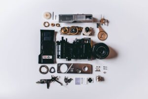
What is a PCB and why is it important?
A PCB, short for printed circuit board, is a crucial component in many electronic devices. It serves as a platform for connecting electronic components to build circuits. PCBs are essential because they provide a sturdy foundation for components, ensuring they are connected correctly and securely. Without PCBs, it would be challenging to assemble the complex circuits found in modern electronic devices.

Key steps in the PCB manufacturing process
PCB manufacturing involves several key steps that are crucial to creating a high-quality printed circuit board for your projects. Here are some important stages in the process:
- Designing the PCB layout: This step involves creating a digital blueprint of the circuit board, specifying the placement of components and routing of electrical connections.
- Gerber file generation: Once the layout is finalized, the design data is converted into Gerber files, which contain the necessary information for manufacturing the PCB.
- Selecting materials: Choosing the right materials for the PCB, such as substrate materials and copper foil, is essential to ensure the board’s performance and durability.
- Printed circuit board fabrication: This involves etching the PCB layers, drilling holes for components, and applying solder mask and silkscreen for component identification.
- Component assembly: The components are then assembled onto the PCB using automated or manual processes, depending on the complexity of the board.
- Testing and quality control: Before the PCB can be used in a project, it undergoes rigorous testing to ensure all connections are correct and the board functions as intended.
These steps play a critical role in the PCB manufacturing process and ultimately determine the performance and reliability of your electronic projects.
Understanding the design phase of PCB development
In the design phase of PCB development, engineers create the blueprint for the circuit board. This step involves determining the layout of components, tracing the electrical connections, and ensuring the board meets the project’s requirements. Key points to grasp about this phase include:
- Component Placement: Deciding where each part will go on the board.
- Tracing Connections: Mapping out the paths for electricity to flow between components.
- Requirements Alignment: Ensuring the design meets the project’s functionality and specifications.
Importance of material selection in PCB fabrication
Selecting the right materials for your PCB is crucial for its performance and durability. The material used can impact the electrical properties of your board, its heat dissipation capabilities, and its overall reliability. Here are a few key reasons why material selection in PCB fabrication matters:
- Electrical Performance: The type of material chosen can affect the signal integrity and impedance of your PCB.
- Thermal Management: Proper materials can help in efficiently dissipating heat, which is crucial for the longevity of your board.
- Reliability: Choosing high-quality materials ensures the long-term stability and performance of your PCB.
By carefully considering the materials during the fabrication process, you can optimize the functionality and lifespan of your PCB for your projects.
Techniques for copper patterning and layering
When creating printed circuit boards (PCBs), there are two common techniques for copper patterning and layering, which are crucial stages in the PCB process.
-
Etching: This method involves using chemicals to remove unwanted copper from the board, leaving behind the desired copper traces for the circuit. It is a precise and widely used technique for creating intricate copper patterns on the PCB layers.
-
Silkscreen Printing: In this technique, a thin layer of ink is applied to the PCB through a stencil to create the desired copper pattern on the board. Silkscreen printing is often used for simpler designs and can be cost-effective for small-scale PCB production.
Understanding these techniques is essential for creating functional and reliable PCBs for your projects.
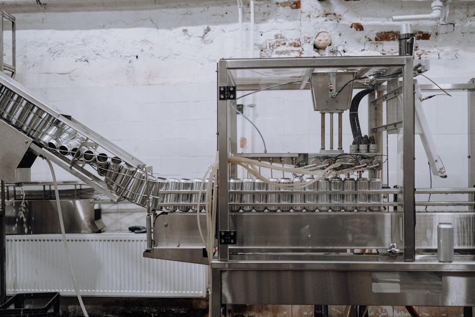
Quality control measures in PCB production
Quality control measures in PCB production ensure the consistency and reliability of each circuit board. Inspections at various stages of the process catch any defects early on, preventing issues down the line. Testing the final product guarantees that it meets the required specifications before moving forward. Adhering to quality standards throughout the production process reduces the likelihood of errors and ensures the functionality and durability of the PCB in your projects.
Soldering and assembly of components on a PCB
Soldering and assembling components on a PCB is a crucial step in creating electronic devices. The process involves carefully attaching electronic parts onto the printed circuit board using solder, which is a metal alloy that melts at high temperatures to form strong connections. Proper soldering ensures that all components are securely in place and that electrical signals can flow smoothly between them. This step is essential for the functionality and durability of your electronic projects.
Testing and inspection methods for PCBs
When it comes to testing and inspecting PCBs, there are several methods used to ensure the quality of the printed circuit board. Some common methods include visual inspection, automated optical inspection, and electrical testing. These methods help identify any defects or issues in the PCB before it is used in a final product. Visual inspection involves closely examining the PCB for any visible defects such as solder bridges or missing components. Automated optical inspection uses cameras and software to detect defects that may not be visible to the naked eye. Electrical testing, on the other hand, checks the functionality of the PCB by sending electrical signals through it. By employing these testing and inspection methods, manufacturers can ensure that the PCBs meet quality standards and function properly in electronic devices.
Factors influencing the cost of PCB fabrication
PCB fabrication costs can vary based on several factors. The complexity of your design plays a significant role in determining the final cost. More complex designs with intricate circuitry may require advanced manufacturing techniques, leading to higher costs. The size and number of layers in your PCB also affect the fabrication cost. A larger PCB with more layers will generally cost more to manufacture. The materials used in your PCB, such as the type of substrate and copper thickness, can impact the overall cost as well. Additionally, the quantity of PCBs ordered can influence the price per unit, with larger quantities often resulting in lower costs per board. Keep these factors in mind when planning your PCB fabrication budget.
Conclusion: The significance of the PCB process for project success
Understanding the significance of the PCB process is crucial for the success of your projects. PCBs are the foundation of electronic devices, acting as a platform for components to connect and function together smoothly. Here’s why the PCB process matters:
- Proper PCB design ensures efficient functionality and connectivity in your electronic projects.
- A well-executed PCB process can result in reduced errors and troubleshooting time during project development.
- Investing time and effort in mastering the PCB process can lead to cost savings and overall project efficiency.
- Ultimately, a thorough understanding of the PCB process can elevate the quality and reliability of your projects.